
Do you have trouble visualizing sizes when doing digital design work or buying things online?
I sure do.
Best solution I've found is also hilariously simple: I keep a retractable tailor's tape within arm's reach of my desk, and whip it out for reference whenever I'm unsure (i.e. almost every time).

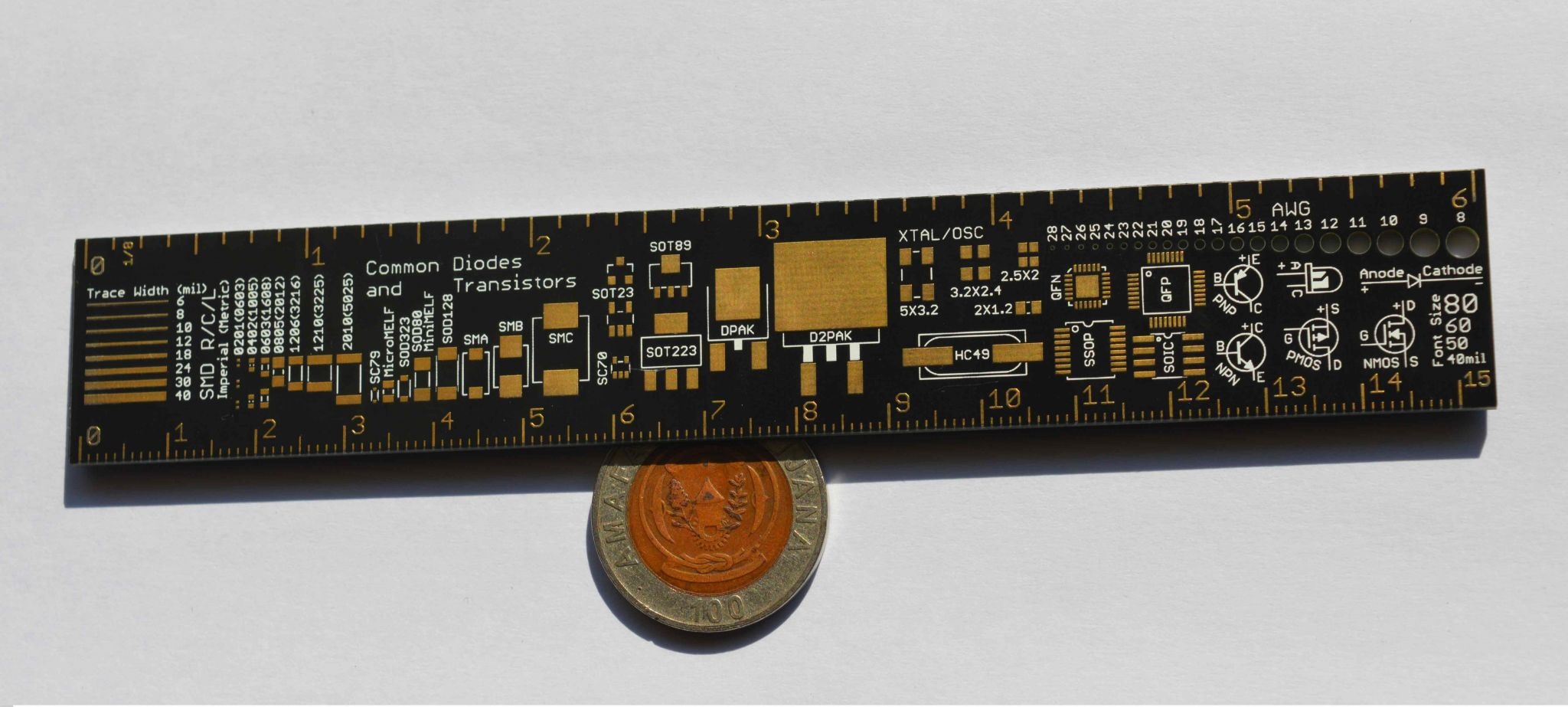
@starkatt This is such a common problem for electrical engineers that you can get these little pcb rulers with actual component footprints on them so you can see what they look like and how they compare to each other
they usually also have other useful stuff on them like trace widths and stuff, too
-F/R
@Felthry I love that ruler, have one myself.
@Felthry 'cause yeah there's no inherent size reference when looking at a PCB layout!